
Preview
基本信息产品详情证书
基本信息
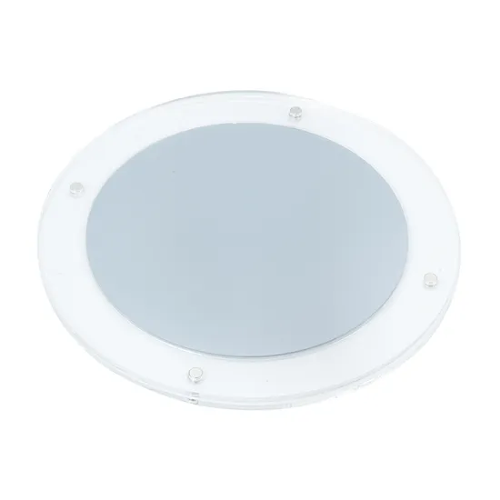
| 型号/编号 | 12英寸 |
| 晶格取向 | 一百 |
| 杂质 | 硼 |
| 电阻率 | 1-100欧姆 |
| 前面部分 | 精炼的 |
| 边缘 | 打磨 |
| 直径 | 300毫米±0.2毫米 |
| 厚度 | 775±25微米 |
| 运输方案 | 半标准 |
| 规格 | TBD |
| 商标 | FSM |
| 起源 | 中国 |
| 商品编码 | 3818001920 |
| 生产能力 | 每月5000件 |
产品详情
Product Description
Preview
Why Choose FSM? - Elevate Your Silicon Wafer Experience
Unmatched Expertise : With a seasoned team of professionals and cutting-edge manufacturing facilities, we consistently deliver wafers of unparalleled quality.Diverse Range of Premium Products : From Czochralski (CZ) and Float Zone (FZ) silicon wafers to SOI and glass wafers, our extensive selection is tailored to meet your precise requirements.Bespoke Customization : We excel in crafting custom wafers to your exacting standards, ensuring the success of your unique projects.Rapid Turnaround Time : Our efficient processes and robust in-stock inventory empower us to deliver swiftly, keeping your projects on track.Extensive Global Reach : Shipping worldwide from our China and Japan warehouses, we serve clients in over 50 countries with excellence.
Unmatched Expertise : With a seasoned team of professionals and cutting-edge manufacturing facilities, we consistently deliver wafers of unparalleled quality.Diverse Range of Premium Products : From Czochralski (CZ) and Float Zone (FZ) silicon wafers to SOI and glass wafers, our extensive selection is tailored to meet your precise requirements.Bespoke Customization : We excel in crafting custom wafers to your exacting standards, ensuring the success of your unique projects.Rapid Turnaround Time : Our efficient processes and robust in-stock inventory empower us to deliver swiftly, keeping your projects on track.Extensive Global Reach : Shipping worldwide from our China and Japan warehouses, we serve clients in over 50 countries with excellence.
Preview
Preview
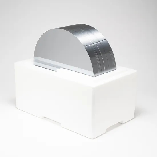
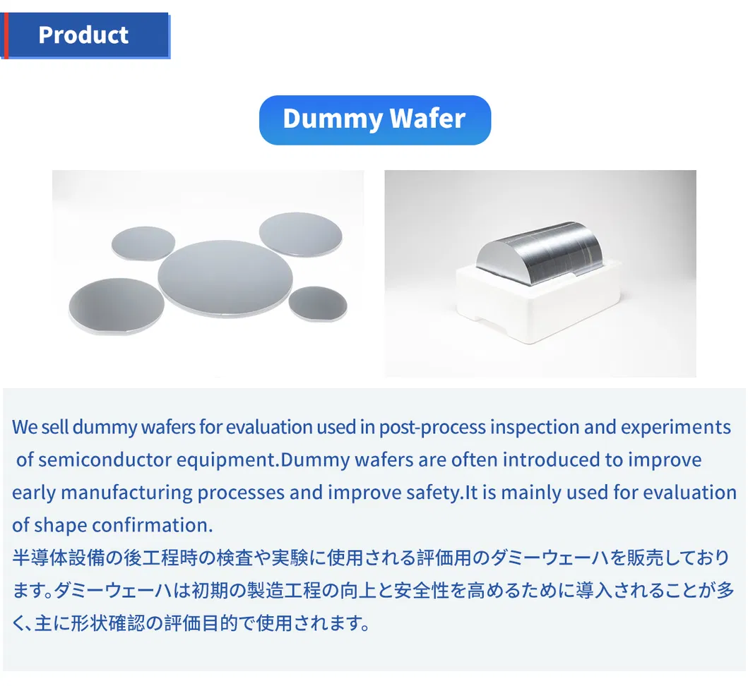
Dummy wafers, also known as test wafers, are primarily utilized for experimentation and testing, distinguishing them from standard product wafers.Consequently, reclaimed wafers are predominantly used as dummy (test) wafers.Dummy wafers are frequently employed in production devices to enhance safety at the initial stage of the production process, as well as for delivery inspection and process evaluation.Given their frequent use in experiments and tests, the size and thickness of dummy wafers are critical considerations.
Preview
Preview
Preview
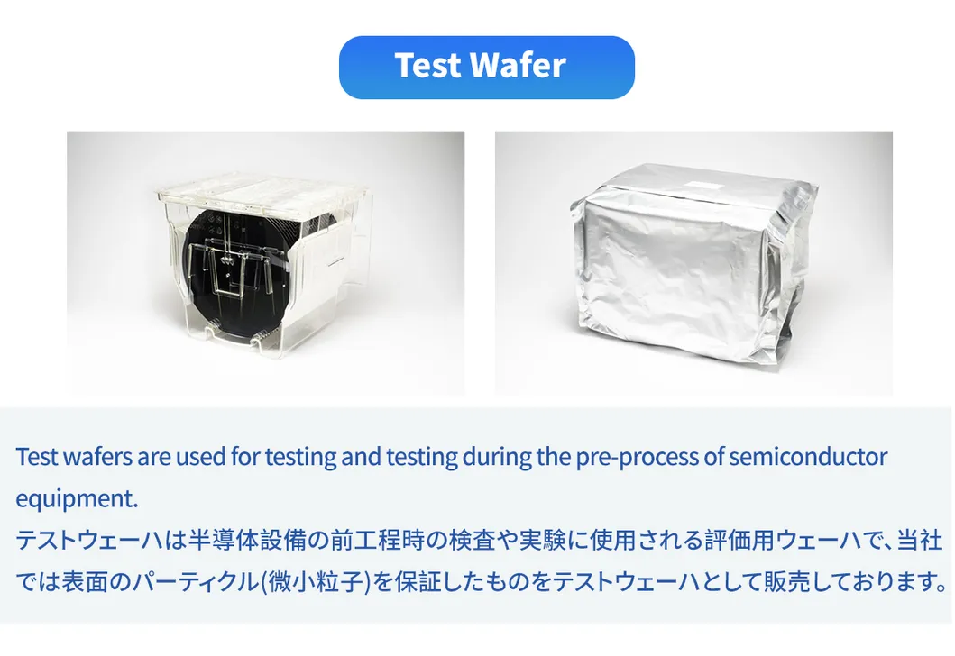
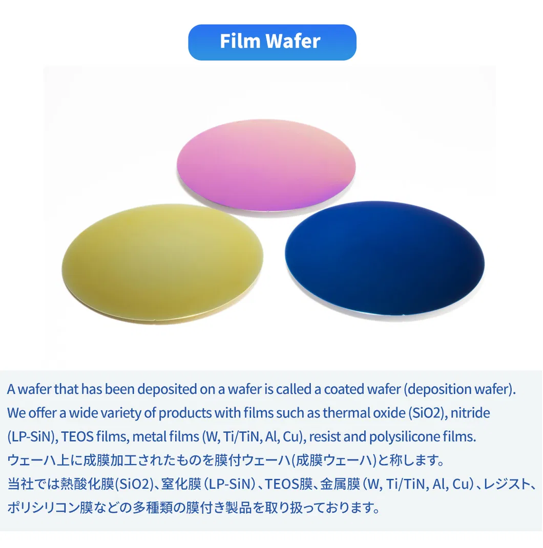
Wafers processed with film deposition are referred to as film wafers.Examples of films used include isolation films for layer separation, metal films for conductivity, and various process materials such as resist and protective films.
Preview
Preview
Preview
Product Parameters
Use Reference Value
150MM/200MM Test Wafer
300MM Test Wafer
200MM/300MM Oxide Wafer
* Please contact us for other film types, film thicknesses, and film compositions.At FSM, we offer the highest quality silicon wafers at competitive prices. Silicon wafers are the primary semiconductor material used in the industry. Our WaferPro silicon wafers provide an unmatched balance of cost and performance.Whether you're seeking to purchase silicon wafers or buy silicon wafers online, our extensive inventory includes SEMI standard silicon wafers in diameters of 2", 3", 100mm, 125mm, 150mm, 200mm, and 300mm, all ready for immediate shipping.For custom wafer sizes or specifications beyond our standard online offerings,contact our team to meet unique semiconductor wafer requirements through our extensive supply chain partnerships.
Preview
Certifications
Preview
Preview
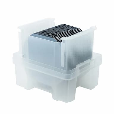
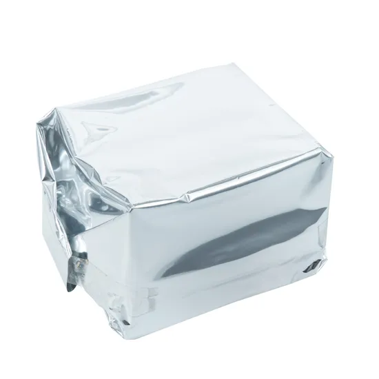
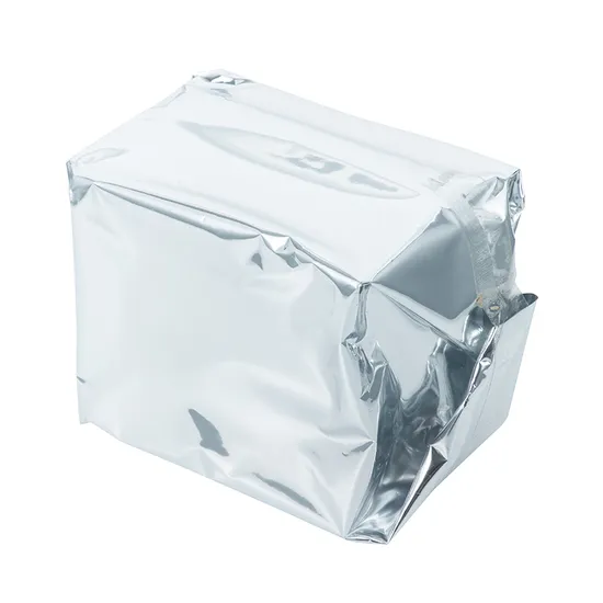
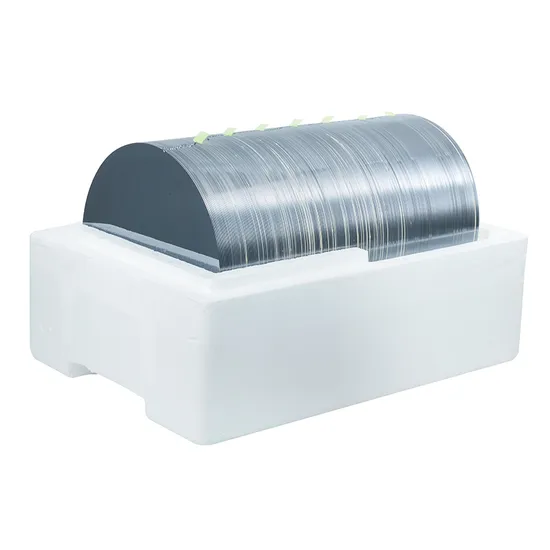
Packaging & Shipping
Preview

Preview
Company Profile
Preview

Preview
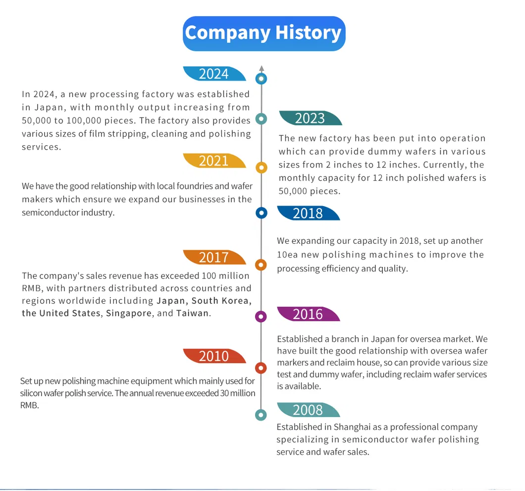
Founded in August 2008, Fine Silicon Manufacturing (Shanghai) Ltd. proudly established a state-of-the-art wafer reclaim factory in the vibrant Shanghai Pudong New Area. Our advanced facility offers high precision lapping and polishing services for wafers ranging from 6 to 12 inches, boasting an impressive capacity of 50,000 pieces per month. In addition, we serve as a valued agent for particle-controlled test wafers reclaim, wafer film coating, and wafer thinning services. Interested in learning more? Please CONTACT US for further information and to explore how we can meet your specialized silicon wafer needs.
Preview
Preview
Our Advantages
Preview
Preview
Preview
FAQ
Preview
Q: What are the available shipping methods?A: We offer a variety of shipping options including DHL, FedEx, ***, UPS, EMS, SF, and others.Q: What payment methods do you accept?A: We accept T/T (Telegraphic Transfer) and PayPal as payment methodsamong several others.Q: What is the delivery timeframe?A: For items in inventory, the delivery time is typically within 5 working days.For customized products, the delivery time ranges from 7 to 25 working days, depending on the order quantity.Q: Is it possible to customize products according to my needs?A: Absolutely! We can customize the material, specifications, and optical coating of our optical components to meet your specific requirements.Every customer's specifications are unique, and Fine Silicon Manufacturing (Shanghai) Ltd. can supply wafers tailored precisely to your needs.If you do not find the exact specifications you require, please
CONTACT FSM
to speak with a member of our experienced and knowledgeable sales team.
CONTACT FSM
to speak with a member of our experienced and knowledgeable sales team.
Preview
证书
标题:SGS认证证书

Preview


 上海
上海  已认证
已认证