
Preview
基本信息产品详情证书
基本信息
| 型号编号 | 12 英寸 |
| 增长法 | CZ |
| 晶体取向 | 一百 |
| 杂质 | 硼 |
| 电阻率 | 1-100欧姆 |
| 前面部分 | 光滑的 |
| Edge | 经过打磨 |
| 直径 | 300±0.2毫米 |
| 厚度 | 775±25微米 |
| 交通运输政策包 | 半标准 |
| 规格 | TBD |
| 商标 | FSM |
| 起源 | 中国 |
| 商品编码 | 3818001920 |
| 生产能力 | 每月五千个/月 |
产品详情
Product Description
Preview
Why Choose FSM?
Expertise: With a team of experienced professionals and state-of-the-art manufacturing facilities, we deliver consistently high-quality wafers.Wide Range of Products: From Czochralski (CZ) and Float Zone (FZ) silicon wafers to SOI and glass wafers, we offer a comprehensive selection to meet your specific needs.Customization: We specialize in manufacturing custom wafers to your exact specifications, ensuring your project's success.Fast Turnaround: Our streamlined processes and in-stock inventory enable us to provide quick delivery, keeping your projects on schedule.Global Reach: We ship worldwide from our China and Japan warehouse, serving customers in over 50 countries.
Expertise: With a team of experienced professionals and state-of-the-art manufacturing facilities, we deliver consistently high-quality wafers.Wide Range of Products: From Czochralski (CZ) and Float Zone (FZ) silicon wafers to SOI and glass wafers, we offer a comprehensive selection to meet your specific needs.Customization: We specialize in manufacturing custom wafers to your exact specifications, ensuring your project's success.Fast Turnaround: Our streamlined processes and in-stock inventory enable us to provide quick delivery, keeping your projects on schedule.Global Reach: We ship worldwide from our China and Japan warehouse, serving customers in over 50 countries.
Preview
Preview
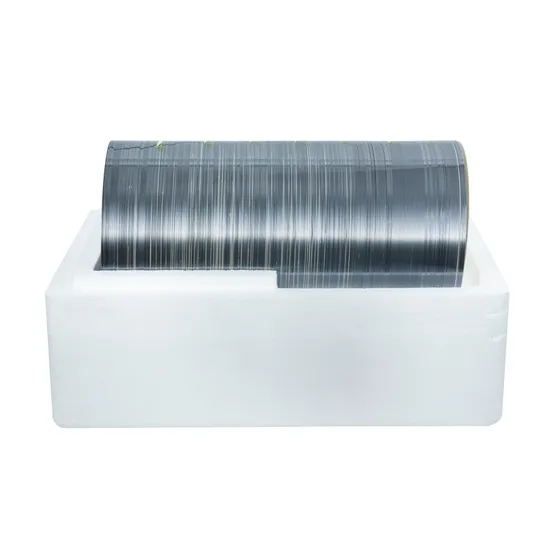
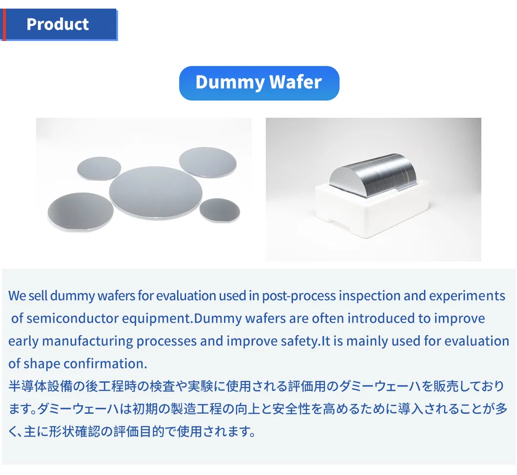
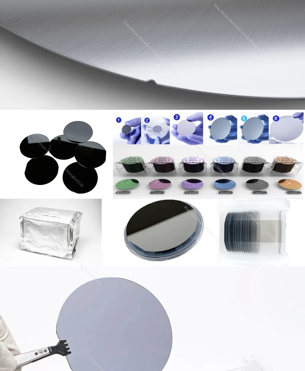
Dummy wafers (also called as test wafers) are wafers mainly used for experiment and test and being different from general wafers for product.
Accordingly, reclaimed wafers are mostly applied as dummy wafers (test wafers).
Dummy wafers are often used in a production device to improve safety in the beginning of production process and are used for delivery check and evaluation of process form.
As dummy wafers are often used for experiment and test, size and thickness thereof are important factors in most occasions.
Preview
Preview
Preview
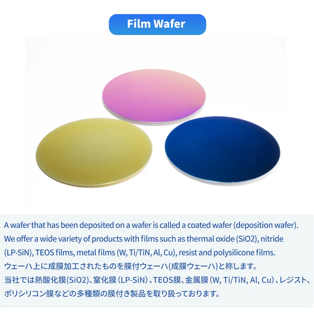
Wafers processed with film deposition is called film wafer.
Examples of film to be used (growth of film) include isolation film as isolation material between layers, metal film as conductive material, process material such as resist and protective film.
Examples of film to be used (growth of film) include isolation film as isolation material between layers, metal film as conductive material, process material such as resist and protective film.
Preview
Preview
Preview
Product Parameters
Use reference value
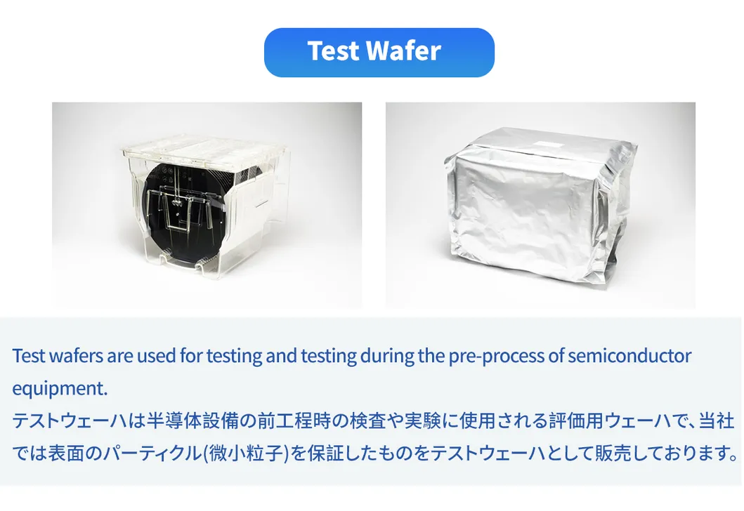
150MM/200MM Test wafer
300MM Test wafer
200MM/300MM Oxide wafer
*
Please contact us for other film types, film thickness, and film composition.
Use reference value
150MM/200MM Test wafer
300MM Test wafer
200MM/300MM Oxide wafer
*
Please contact us for other film types, film thickness, and film composition.
Preview
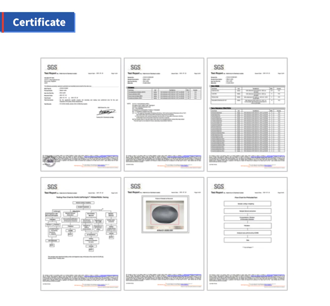
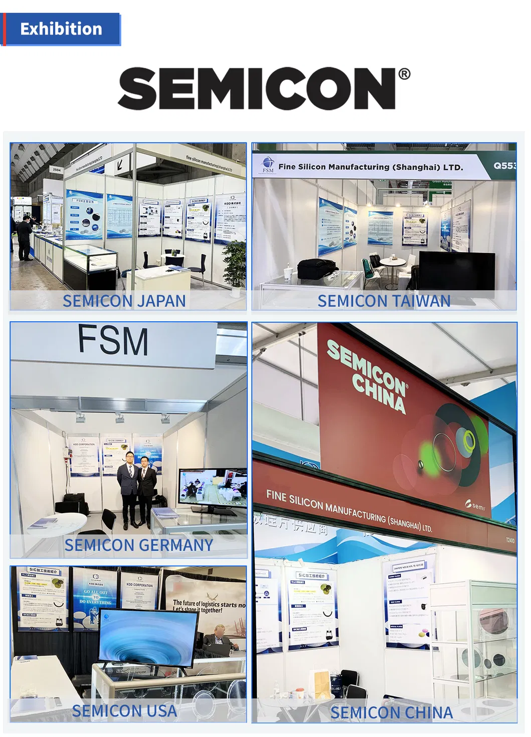
Certifications
Preview
Preview
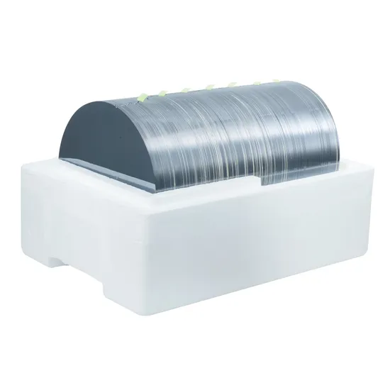
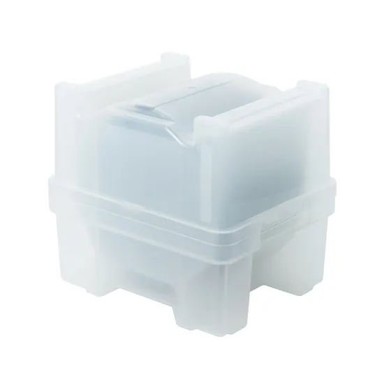
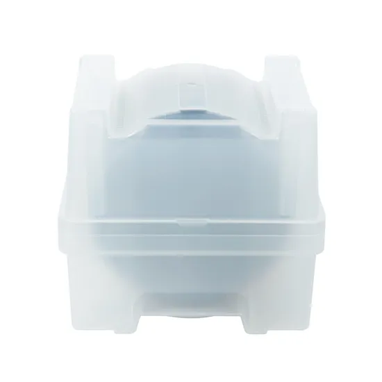
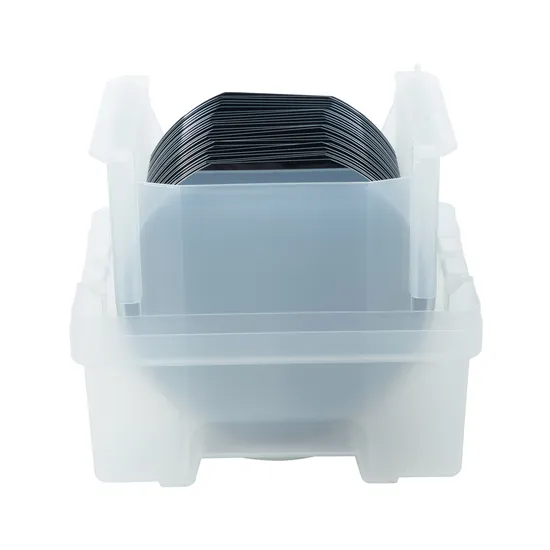
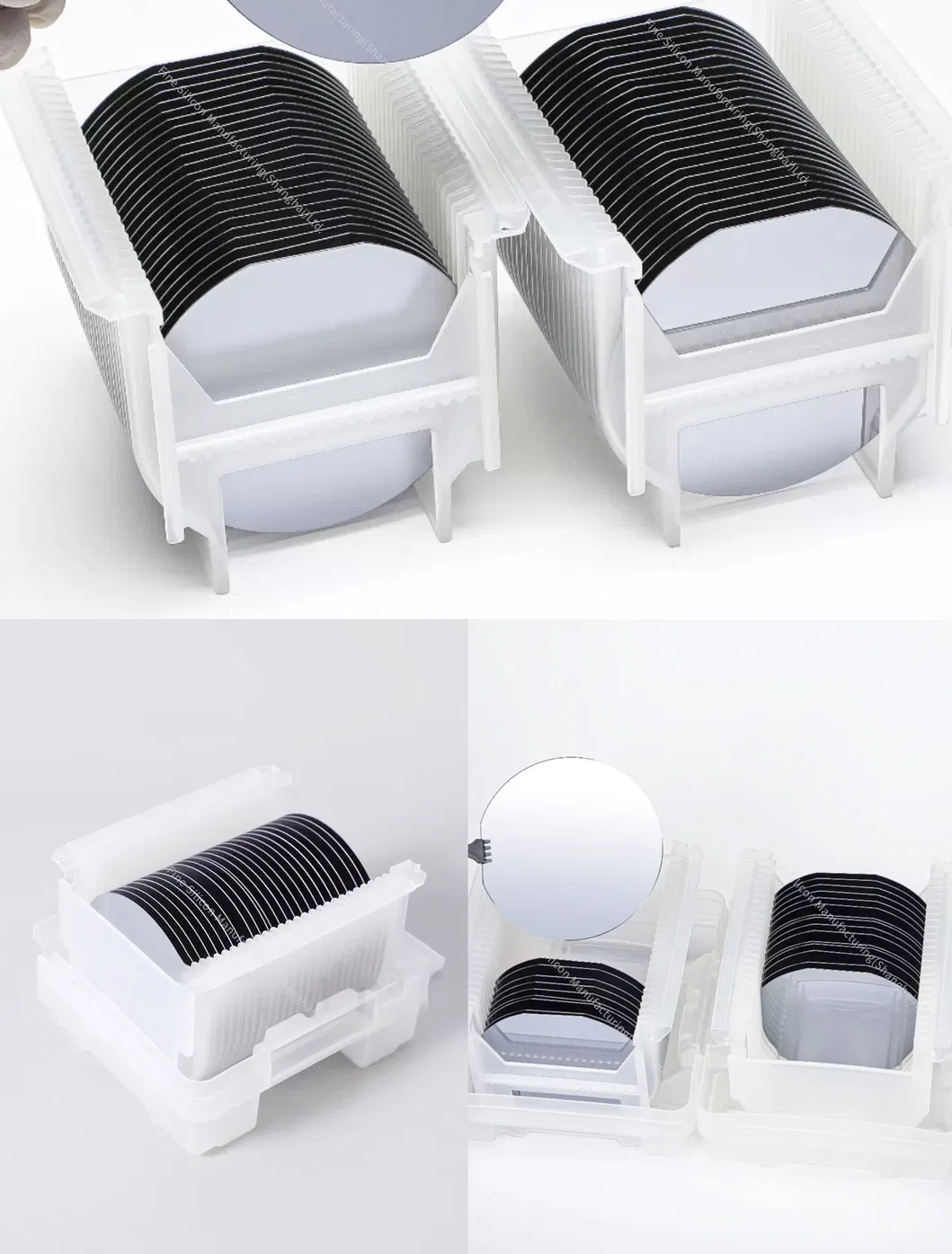
Packaging & Shipping
Preview

Preview
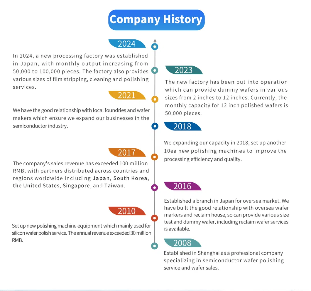
Company Profile
Preview

Preview
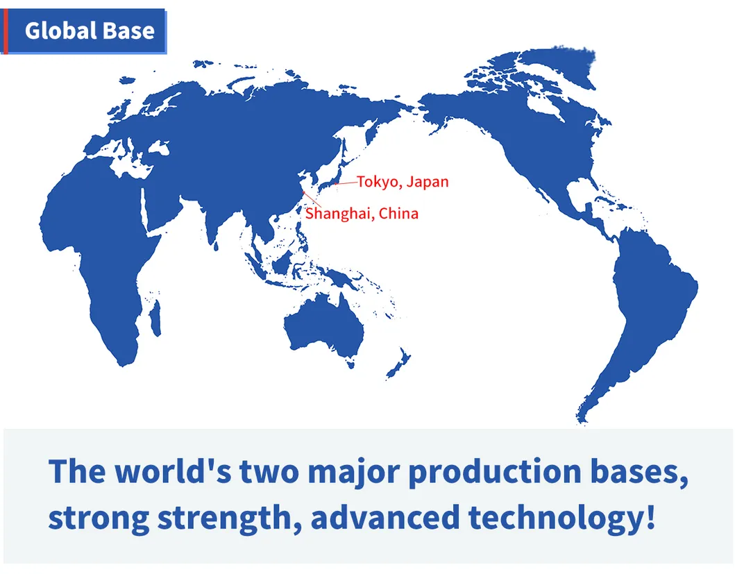
Fine Silicon Manufacturing(Shanghai) Ltd. was established in August, 2008. We built a wafer reclaim factory in Shanghai Pudong New Area,
providing mainly 6-12inch wafers lapping and polishing. 50K PCS/month capacity. Meanwhile, we are the agent of particle controlled test wafers reclaim, wafer film coating, wafer thinning. If you have interest, PleaseCONTACT USfor more information.
providing mainly 6-12inch wafers lapping and polishing. 50K PCS/month capacity. Meanwhile, we are the agent of particle controlled test wafers reclaim, wafer film coating, wafer thinning. If you have interest, PleaseCONTACT USfor more information.
Preview
Preview
Our Advantages
Preview
Preview
Preview
FAQ
Preview
Q: What's the way of shipping ?
A:
We accept DHL, Fedex, TNT, UPS, EMS, SF and etc.
Q: How to pay?
A:
T/T, PayPal
and etc..
Q: What's the deliver time?
A:
For inventory: the delivery time is 5 workdays.
For customized products: the delivery time is 7 to 25 workdays. According to the quantity.
Q: Can I customize the products based on my need?
A:
Yes, we can customize the material, specifications and optical coating for your optical components based on your needs.
Every customer's specification is unique and FSM can supply wafers that meet your exact specifications.
If you do not see the specification you require, please
CONTACT FSM
to speak with a member of our experienced and knowledgeable sales staff.
A:
We accept DHL, Fedex, TNT, UPS, EMS, SF and etc.
Q: How to pay?
A:
T/T, PayPal
and etc..
Q: What's the deliver time?
A:
For inventory: the delivery time is 5 workdays.
For customized products: the delivery time is 7 to 25 workdays. According to the quantity.
Q: Can I customize the products based on my need?
A:
Yes, we can customize the material, specifications and optical coating for your optical components based on your needs.
Every customer's specification is unique and FSM can supply wafers that meet your exact specifications.
If you do not see the specification you require, please
CONTACT FSM
to speak with a member of our experienced and knowledgeable sales staff.
Preview
证书
标题:SGS认证证书

Preview


 上海
上海  已认证
已认证