Product


Preview
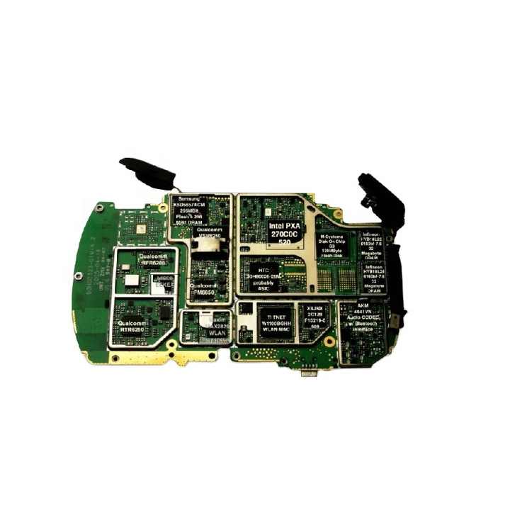
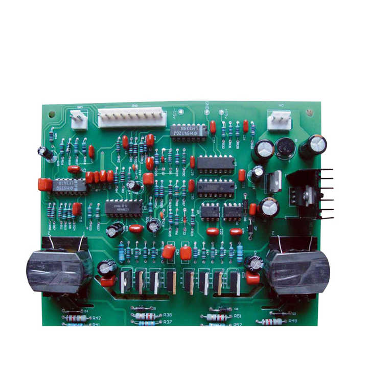
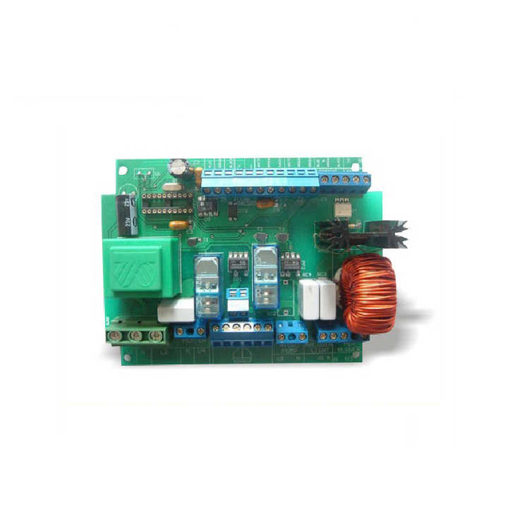
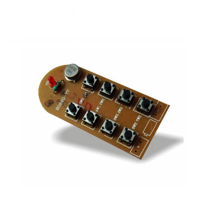
Basic Info.Product Description
Basic Info.
| Number of Layers | 4-layer |
| Base Material | FR4 |
| Board Thickness | 1.6mm |
| Board Size | Multilayer PCB |
| Model Number | TH-20210616-005 |
| Type | Multilayer pcb |
| Place of Origin | Guangdong, China |
| Brand me | TH |
| Copper Thickness | 1oz |
| Min. Hole Size | 0.2mm |
| Min. Line Width | 0.1mm |
| Min. Line Spacing | 0.1mm |
| Surface Finishing | Hasl |
| Solder Mask | Green,Blue |
| Silkscreen | White |
| Electronic Test | Test-rig |
| Selling Units: | Single item |
| Single package size: | 10X10X4 cm |
| Single gross weight: | 0.500 kg |
Product Description
ItemSpecification
1NumbrofLayer1-18Layers
2MaterialFR-4,FR2.Taconic,Rogers,CEM-1CEM-3,ceramic,crockeryMetal-backedLaminate
3SurfaceFinishHASL(LF),Goldplating,Electrolessnickelimmersiongold,ImmersionTin,OSP(Entek)
4FinishBoardThickness0.2mm-6.00mm(8mil-126mil)
5CopperThickness1/2ozmin;12ozmax
6SolderMaskGreen/Black/White/Red/Blue/Yellow
7Min.TraceWidth&LineSpacing0.075mm/0.1mm(3mil/4mil)
8Min.HoleDiameterforCNCDriling0.1mm(4mil)
9Min.HoleDiameterforpunching0.9mm(35mil)
10Biggestpanelsize610mm*508mm
11HolePositon+/-0.075mm(3mil)CNCDriling
12ConductorWidth(W)
0.05mm(2mil)or;
+/-20%oforiginalartwork
13HoleDiameter(H)
PTHL:+/-0.075mm(3mil);
Non-PTHL:+/-0.05mm(2mil)
14OutlineTolerance
0.125mm(5mil)CNCRouting;
+/-0.15mm(6mil)byPunching
15Warp&Twist0.70%
16InsulationResistance10Kohm-20Mohm
17Conductivity<50ohm
18TestVoltage10-300V
19PanelSize110×100mm(min);660×600mm(max)
20Layer-layermisregistration
4layers:0.15mm(6mil)max;
6layers:0.25mm(10mil)max
21Min.spacingbetweenholeedgetocircuitypqtternofaninnerlayer0.25mm(10mil)
22Min.spacingbetweenboardoulinetocircuitrypatternofaninnerlayer0.25mm(10mil)
23Boardthicknesstolerance
4layers:+/-0.13mm(5mil);
6layers:+/-0.15mm(6mil)
24ImpedanceControl+/-10%
25DifferentImpendance+-/10%
Q1.WhatdoweneedforPCBorPCBAquotation?
PCB:Gerberfiles/PCBfiles,Quantity,Boardprocessingdetails(boardmaterial,thickness,copperthickness,surfacetreatment,colorofsoldermaskandsilkscreen)
PCBA:AbovePCBinfo,BOMwithcomponentsspecs,testingdocifyouhave
Q2.DowehaveMOQ?
ThereisnoMOQinTAILHOO.WeareabletoproduceSmallvolumeaswellaslargevolumeproductionwithflexibility.
Q3.Aremyfilessafe?
Yes.Allofourclient’sdesignfilesareclassifiedandsafe.Andwe’llnotsharewiththirdparty.IfNDAneeded,we’llsign.
Q4.Iftheproductfailsafterreceive,whatshouldIdo?
Wewillberesponsibleforalloftheproductwesendout.Ifyouhavesentustestdocs,we’llgurantee0%defectiverate,whichmeansifyoureceivedefectiveones,wewillberesponsibleforit.Ifyoudon’thavetestdocs,we’llgurantee0.3%defectiverate.
Q5,IfIonlyhavesamples,canIproduceit?
Yes.Wecancopyitandproducebasedonyoursamples.
Q6.Shippingcost?
Theshippingcostisdependonthedestination,weight,packingdimension.Wecanquoteyouwhenproductionfinish,orevenbeforeproductionstarting.

Preview
Custom circuit board prototype multilayer pcb pcba assembly manufacturer
$0.35 ~ $1.68
Consumer electronics Industry Chain · printed circuit board · Multilayer PCB


 Shenzhen
  Authenticated
Less than 50 EmployeesWholesale/Retail/New Retail