Product
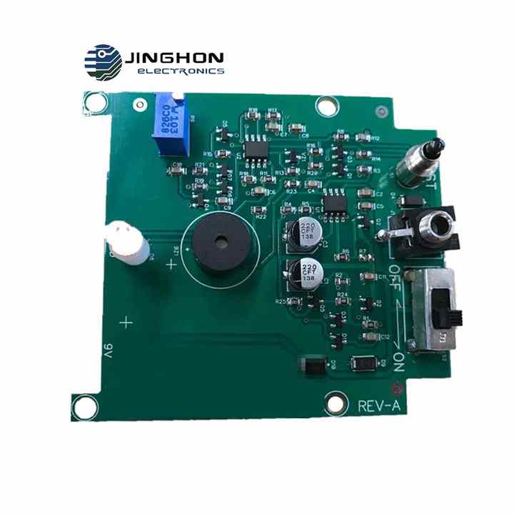

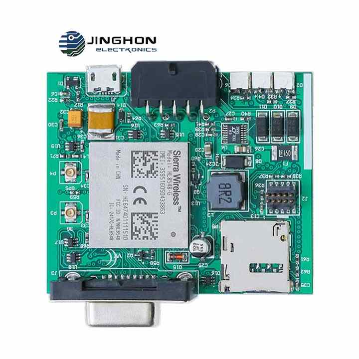
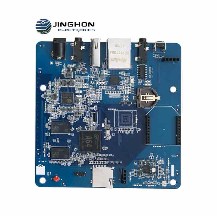
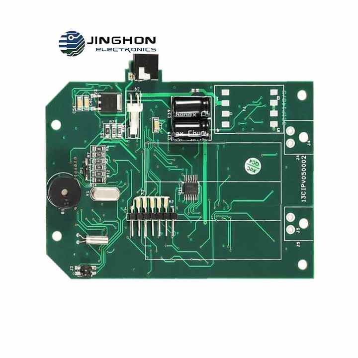

Preview
Basic Info.Product Description
Basic Info.
| Base Material | FR-4 |
| Board Thickness | 1.6mm |
| Model Number | Customized |
| Type | metal core pcb |
| Place of Origin | Guangdong, China |
| Brand Name | Jinghon |
| Copper Thickness | 1OZ |
| Min. Hole Size | 0.10mm |
| Min. Line Width | 0.10mm |
| Min. Line Spacing | 0.075mm |
| Surface Finishing | HASL/Lead Free HASL/ENIG |
| Board Size | OEM |
| Product name | Metal Core PCB |
| Solder mask color | Green Blue Black |
| Way of shipping | DHL/UPS/EMS/Feldex |
| Package | vacuum package |
| MOQ | 1piece |
| Service | EMS/OEM |
| Certification: | ISO9001 |
| Layer Count | 1-24 Layer |
| Test | Flying probe test /test fixture |
| Packaging Details | anti-static package inside and standard carton outside. |
| Selling Units: | Single item |
| Single package size: | 5X4X3 cm |
| Single gross weight: | 2.000 kg |
| Supply Ability | 30000 Square Meter/Square Meters per Month |
Product Description
PCB Item
Manufacture Capacity
Layer Counts
1--40L
Base Material:
FR4,High-TG FR4,Halogen free,aluminum,High Frequency(Taconic,Aron,PTFE,F4B)
Max board size(mm)
1200x400mm
Board Thickness
0.4mm--7mm
Minimum line/space
0.075mm
Min Hole Size(mechanical)
0.15mm
Min Hole Size(laser hole)
0.1mm
Copper Weight
0.5--6oz
Surface Finish
HAL,lead-free HAL,ENIG,Plated Gold,Immersion Gold,OSP
Solder Mask
Green, Blue, Black, White, Yellow, Red, Matt Green, Matt Black, Matt Blue
Silkscreen
White, Black, Blue,Yellow
Acceptable File Format
Gerber file,Powerpcb,CAD,AUTOCAD,ORCAD,P-CAD,CAM-350,CAM2000
Outline profile
Rout/ V-cut/ Bridge/ Stamp hole
FPC Item
TECHNICAL PARAMETER
Layers
1-6 Layers
Mini thickness
0.08mm
Min.Line Width
0.05mm
Min.Hole Size
0.15mm PTH
Min. PTH Hole Ring
0.45mm
Min. Gap between Cover Layer and Pad
0.1mm
Min. Gap between Trace and Outline
0.2mm
Trace Width Tolerance
±0.03mm W±30%
Outline Tolerance
±0.05mm L≤25mm
Hole Size Tolerance
±0.05mm
Stiffener and Outline Tolerance
±0.1mm
Surface Treatment
ENIG,Gold Plating,HAL,Plating Pb-Sn
PCBA Item
TECHNICAL PARAMETER
Stencil size/range:
736x736mm
Minimum IC pitch:
0.30mm
Maximum PCB size:
1200x 500mm
Minimum PCB thickness:
0.35mm
Minimum chip size:
0201 (0.2x0.1)/0603 (0.6 x 0.3mm)
Maximum BGA size:
74x74mm
BGA ball pitch:
1.00mm (minimum), 3.00mm (maximum)
BGA ball diameter:
0.40mm (minimum), 1.00mm (maximum)
QFP lead pitch:
0.38mm (minimum), 2.54mm (maximum)
Frequency of stencil cleaning:
1 time/5 to 10 pieces
Delivery Time
Sample Lead Time
Mass Production Lead time
Single Sided PCB
1-2 Days
4-7 Days
Double Sided PCB
2-4 Days
7-10 Days
Multilayer PCB
5-8 Days
10-15 Days
PCB and Assembly
8--15 Days
15--20 Days
Sample Lead Time
Mass Production Lead time
Single Sided PCB
1-2 Days
4-7 Days
Double Sided PCB
2-4 Days
7-10 Days
Multilayer PCB
5-8 Days
10-15 Days
PCB and Assembly
8--15 Days
15--20 Days
FAQ
Shenzhen Fast Delivery Pcb Pcba Samples Export Company
$0.3
Consumer electronics Industry Chain · printed circuit board · Metal Core PCB


 Shenzhen
  Authenticated
Less than 50 EmployeesWholesale/Retail/New Retail